First reflow soldering attempt
My current SCSI2SD project design includes a QFN (no-leads) part, which makes hand soldering impossible. The normal method of soldering these parts is via "reflow" in a purpose-built commercial oven that follows very strict temperature profiles. I don't have such an oven, but the good people at sparkfun convinced me that a simple kitchen applicances will suffice.
I purchased:
- A 1800W hotplate ($19 from Sams Warehouse. Cheaper than the skillets.)
- A syringe of no-clean solder paste from Jaycar
The hotplate surface was not smooth like a skillet, and I decided this would make life difficult. Various forum posts recommeded the use of a thick aluminium plate, but alas I couldn't find such a thing at the hardware store. So I bought a $4 very thin aluminium (I ithink) pizza tray from a discount store.
Step 1 - Apply Solder Paste
This isn't too difficult; just squeeze some paste on the pad, and drop an SMD device on. It's not necessary to be exact with the paste or placement as the suface tension of the solder will pull everything on to the pads when melted. I ran continuous beads across all of the IC pins, but as you can see below, I applied way too much. A VERY narrow bead is all that is required for small-pitch devices.
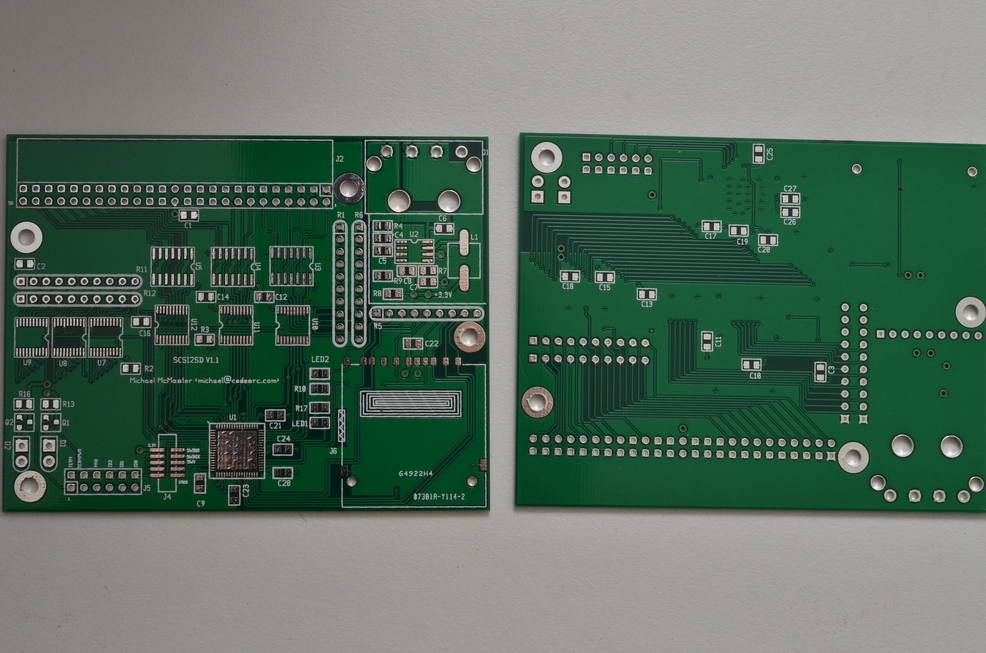 - bare PCB
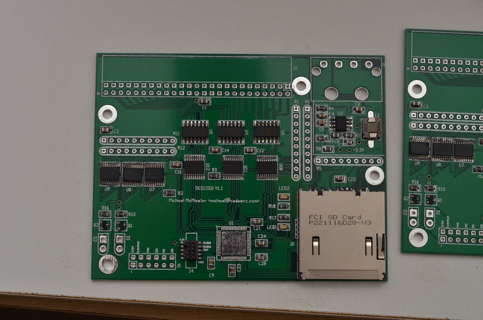 - paste and components applied.
My entire reason for choosing the reflow method was to solder the QFN64 part. Unfortunately I used a QFN68 10x10mm footprint instead of an 8x8mm footprint. I left the placement of this component until last because it requires a fair amount of paste on the exposed-pad, and I wasn't entirely sure how long my tube of paste would last. I hadn't previously checked the layout because digikey placed it in a bag with many warnings about being a moisture-sensitive component, and not to open the bag until I was ready to solder it. At the point where I found out my PCB is useless I'd already placed the other components, so I decided I may as well reflow it as an educational exercise.
Step 2 - Apply heat
My reflow profile consisted of "turn hotplate on, wait for solder to melt, turn hot plate off.". Sounds simple, right ?
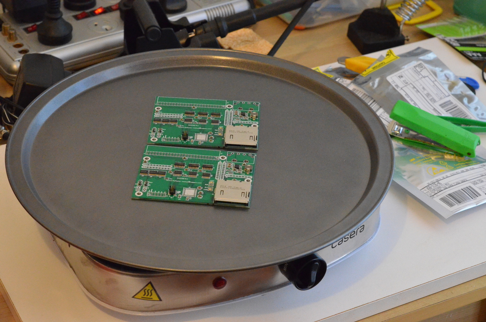 - ready for reflow.
Notice in the above pic how the PCB is sitting nice and level on the pizza tray. This was intentional. Unfortunately the tray deformed almost the instant I turned the hotplate on. This was bad; only a small area of the PCBs were touching the metal surface beneath.
I waited for the paste to melt. While I waited, I noticed a corner of a PCB started to bubble, and then melt. It smelt very bad. Determined to learn whether my solder paste application was correct, I did not turn the hot plate off until all of the solder paste at the "cold" end of the boards had melted.
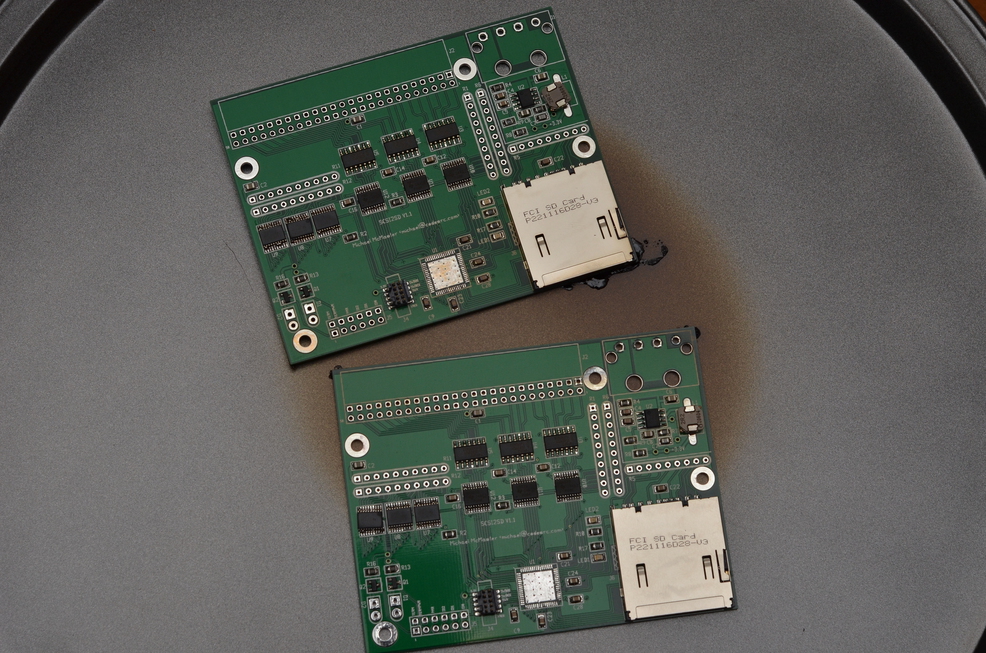 - the result.
The black material around the PCBs is melted PCB. I have a feeling these particular devices will never work.
Ignore the mis-placement of the inductor of the upper-right corner. I accidentally nudged this when trying to reposition the PCB on the pizza tray so there was more contact between them.
The 0808, SOIC devices, and SD card holder reflowed perfectly. The fine-pitch TSSOP packages did not - there are many solder bridges, and one part is not aligned correctly. I think these issues are due to an excess of solder paste.
Lessons Learnt
- Use a stencil to ensure the correct amount of solder paste is applied. The syringe works well for the larger pitch components, but it is hard to apply a reduced amount to fine-pitched parts.
- Use a THICK aluminium plate on the hotplate. Ensure this metal won't warp or bend due to the heat. Probably best to check this before doing the reflow!
Notes to self
- Reduce pad length of the inductor footprint.
- Change PCB layout to use 8x8 QFN 64 footprint
- Move J2 over to the right 1-2mm (so the right edge of the silkscreen is where the mounting hole starts. Remove mounting hole).
- J1 is facing the wrong way.
- Put some silk screen marks on J4 to indicate orientation wrt to the tab on the socket.
- Silkscreen orientation marks for the leds (indicate negative pad)